PN JUNCTION BASICS
(1) A p-n junction is a boundary or interface between two types of semiconductor materials, p-type and n-type, inside a single crystal of semiconductor. The "p" (positive) side contains an excess of holes, while the "n" (negative) side contains an excess of electrons in the outer shells of the electrically neutral atoms there. This allows electrical current to pass through the junction only in one direction. The p-n junction is created by doping
(2) p-n junctions are elementary "building blocks" of semiconductor electronic devices such as diodes, transistors, solar cells, light-emitting diodes (LEDs), and integrated circuits.
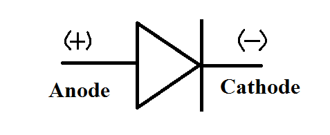
* Symbol for PN junction diode is as shown in figure

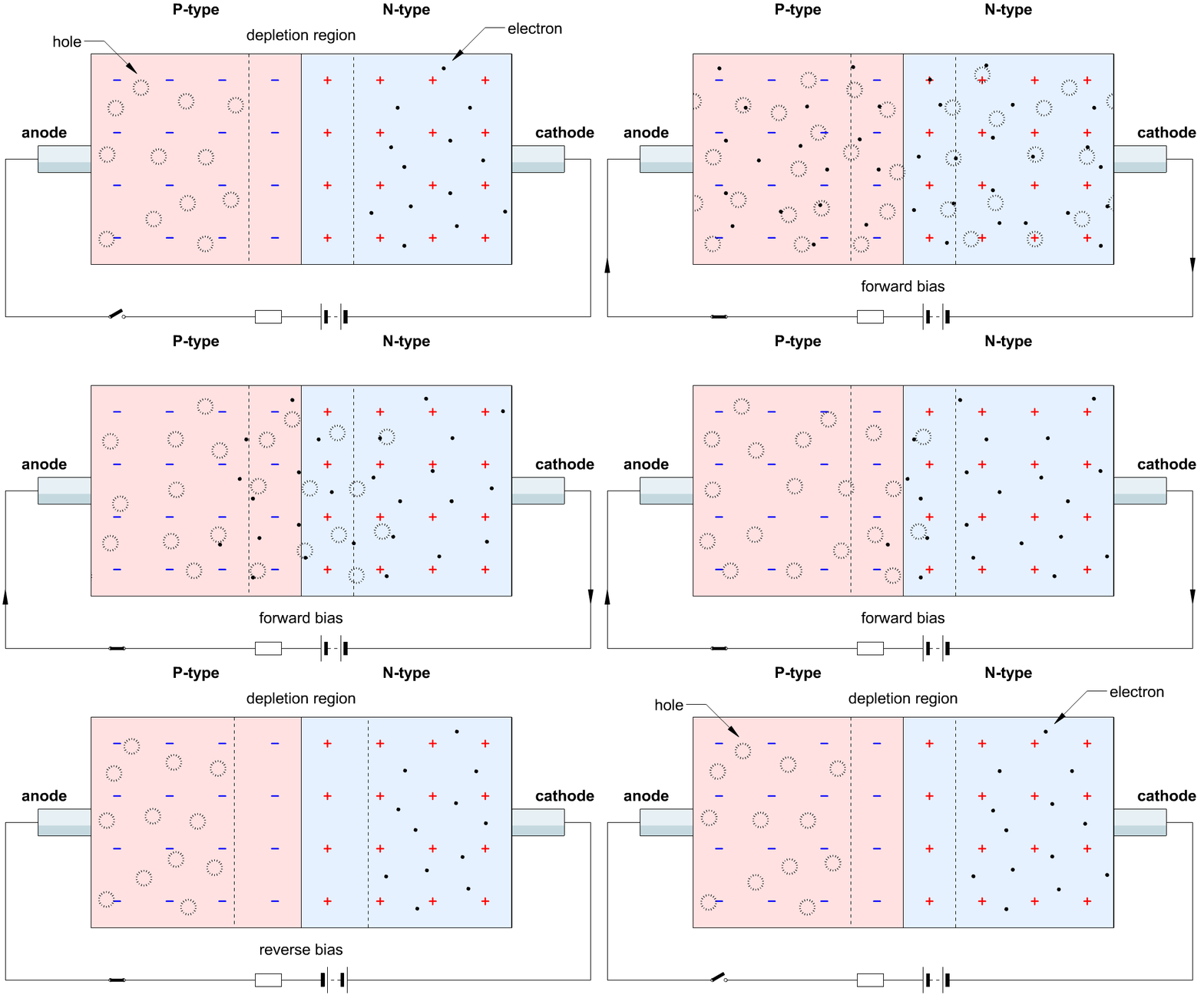
(3) When the p-n junction is formed a few electrons from t he n-type diffuse through the junction and combines with the holes in the p-side to form negative ions and leaves behind positive ions in the n-side. This results in the formation of the depletion layer, which acts as the barrier and does not allow any further flow of electrons from the n region to the p region.

BIASING AN PN JUNCTION
1. Reverse Bias(False connection):
- If a voltage is applied across the diode in such a way that the n-type half of the diode was connected to the positive terminal of the voltage source and the p-type half was connected to the negative terminal.
- Electrons from the external circuit would create more negative ions in the p-type region by "filling the holes" and more positive ions would be created in the n-type region as electrons are displaced toward the positive terminal of the voltage source. hence depletion regions width increases.
2. Forward Bias(True connection):
- If a voltage is applied across the diode in such a way that the n-type half of the diode was connected to the negative terminal of the voltage source and the p-type half was connected to the positive terminal.