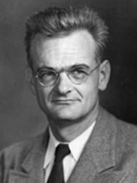
The first person to describe the electrical characteristics of a Zener diode was Clarence Melvin Zener. Theoretical physicist Clarence Zener was employed by Bell Labs. His contributions led to the Zener diode being named in his honour. In a study written in 1934, he originally proposed the breakdown effect that bears his name.
Zener-diode
• As we know, generally In Reverse biasing, Juctions diodes are usually damaged.
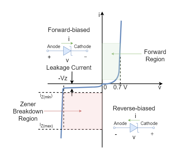
• A Zener Diode, also known as a breakdown diode, is a heavily doped semiconductor device that is designed to operate in the reverse direction.
• When the voltage across the terminals of a Zener diode is reversed and the potential reaches the Zener Voltage (knee voltage), the junction breaks down and the current flows in the reverse direction. This effect is known as the Zener Effect.
• In the forward bias direction, the zener diode behaves like an ordinary silicon diode.
• In a DC circuit, zener diode can be used as a voltage regulator or to provide voltage refrence.
Cause of this electric breakdown
An electrical breakdown of any material such as the conductor, semiconductor, and insulator can occur due to two different phenomena known as
a) Zener Breakdown
b) Avalanche Breakdown
NOTE : When the diode is reverse biased, the kinetic energy of the electrons increases, and they move at a high velocity. The high-velocity electrons collide with other atoms and give rise to free electrons. These free electrons, in turn, give rise to a high value of reverse saturation current. This is known as Zener breakdown.
(a) Zener Breakdown
(i) It occurs in diodes that are highly doped.
(ii) The process in which the electrons move across the barrier from the valence band of p-type material to the conduction band of n-type material is known as Zener breakdown.
(iii) The VI characteristics of a Zener breakdown has a sharp curve.
(iv) The increase in temperature decreases the breakdown voltage.
(b) Avalanche Breakdown
(i) It occurs in diodes that are highly doped.
(ii) The process of applying high voltage and increasing the free electrons or electric current in semiconductors and insulating materials is called an avalanche breakdown.
(iii) The VI characteristic curve of the avalanche breakdown is not as sharp as the Zener breakdown.>
(iv) The increase in temperature increases the breakdown voltage.

- Zener diode behaves as a simple diode (on) when forward-biased.
- Zener diode can acts as a switch (off) when reverse-biased up to Zener Voltage (VZ).
Concept of tunnling diodeIn the case of the tunnel diode, the conditions for tunneling were achieved by more heavily doping the semiconductors associated with the pn junction. With germanium or gallium arsenide the depletion layer at the junction was very narrow, and permitted electrons to tunnel across the barrier. For very low reverse voltages through small positive voltages, the tunneling increased and the junction acted like a conductor.
